Follow us on Google News (click on ☆)
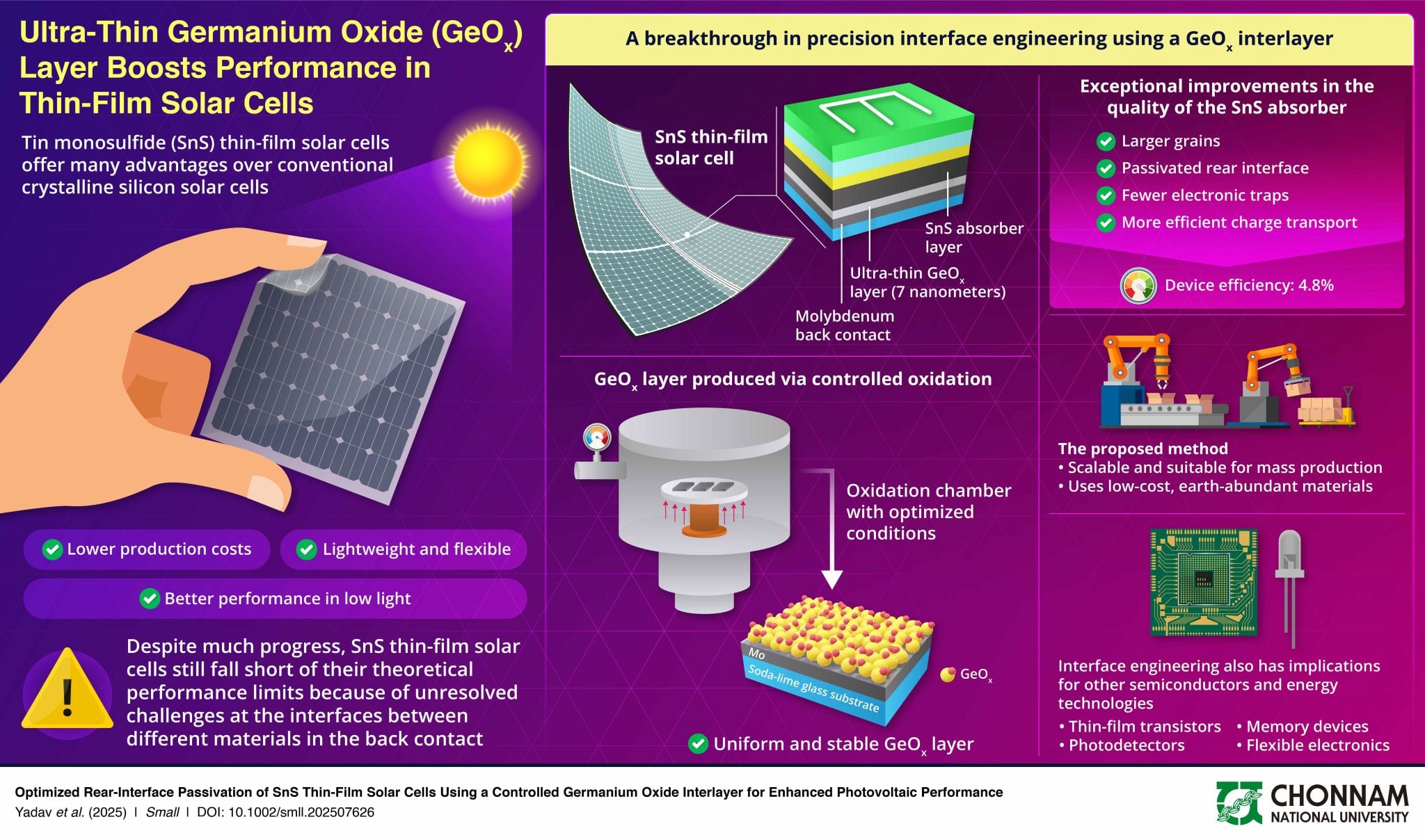
The difficulties are primarily concentrated at the interface between the light-absorbing layer and the rear metal electrode. At this precise location, microscopic defects, unwanted chemical reactions, and atom migration disrupt the flow of electrical charges. Consequently, these disturbances significantly limit the cell's ability to convert sunlight into usable electricity.

Diagram illustrating how the germanium oxide interlayer improves the structure and performance of the solar cell.
Credit: Prof. Jaeyeong Heo, Chonnam National University
Fortunately, a team from Chonnam National University in South Korea has discovered an interesting lead to solve this problem. Their approach consists of inserting an extremely thin layer of germanium oxide, just 7 nanometers thick, between the molybdenum contact and the active tin sulfide layer. This nanometric film acts as a multifunctional shield at the atomic scale.
To achieve this, the researchers used a vapor-phase deposition process, a method compatible with larger-scale production. According to Professor Jaeyeong Heo, this thin interlayer helps block impurity diffusion, prevent the formation of resistive compounds, and reduce defects in the material. As a result, these improvements lead to a more homogeneous structure and more efficient charge transport.
The results published in the journal Small confirm a clear progression. Indeed, the power conversion efficiency increased from 3.71% for standard cells to 4.81% with the new architecture, representing an improvement of nearly 30%! This advance represents one of the highest values ever recorded for tin sulfide-based solar cells manufactured by this technique.
This mastery of the metal/semiconductor interface could have implications far beyond the photovoltaic domain alone. For example, it could benefit other technologies like thin-film transistors, thermoelectric devices, or sensors, where contact quality is crucial for overall performance. This work thus opens new perspectives for the development of advanced electronic components.
How a thin-film solar cell works
Unlike conventional crystalline silicon panels, thin-film solar cells are distinguished by their reduced thickness, often less than a micrometer. Their fabrication relies on depositing thin layers of photovoltaic materials onto a glass, plastic, or metal substrate. This approach allows for faster and less energy-intensive production, with lower use of raw materials.
Their basic principle remains the conversion of light into electricity via the photovoltaic effect. When photons from sunlight strike the semiconductor material, they release electrons, creating an electric current. However, the thinness of the layers requires great precision in manufacturing to avoid energy losses.
Among the materials used are cadmium telluride or amorphous silicon. Tin sulfide attracts attention for its abundance and lack of toxicity. These cells are particularly suited for applications requiring flexibility or discrete integration, such as on buildings or connected objects.